Using the KiCad Footprint Wizard
For demonstration we will be using the KiCad Footprint wizard to generate a footprint for LM317BT.
Open KiCad and Footprint Editor.
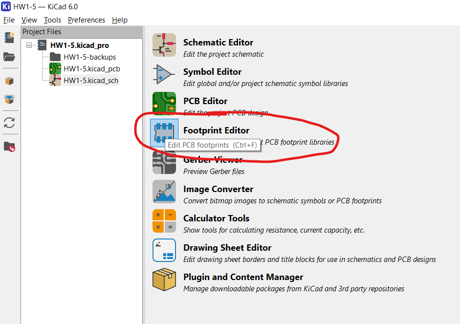 Figure
Open the Footprint Wizard.
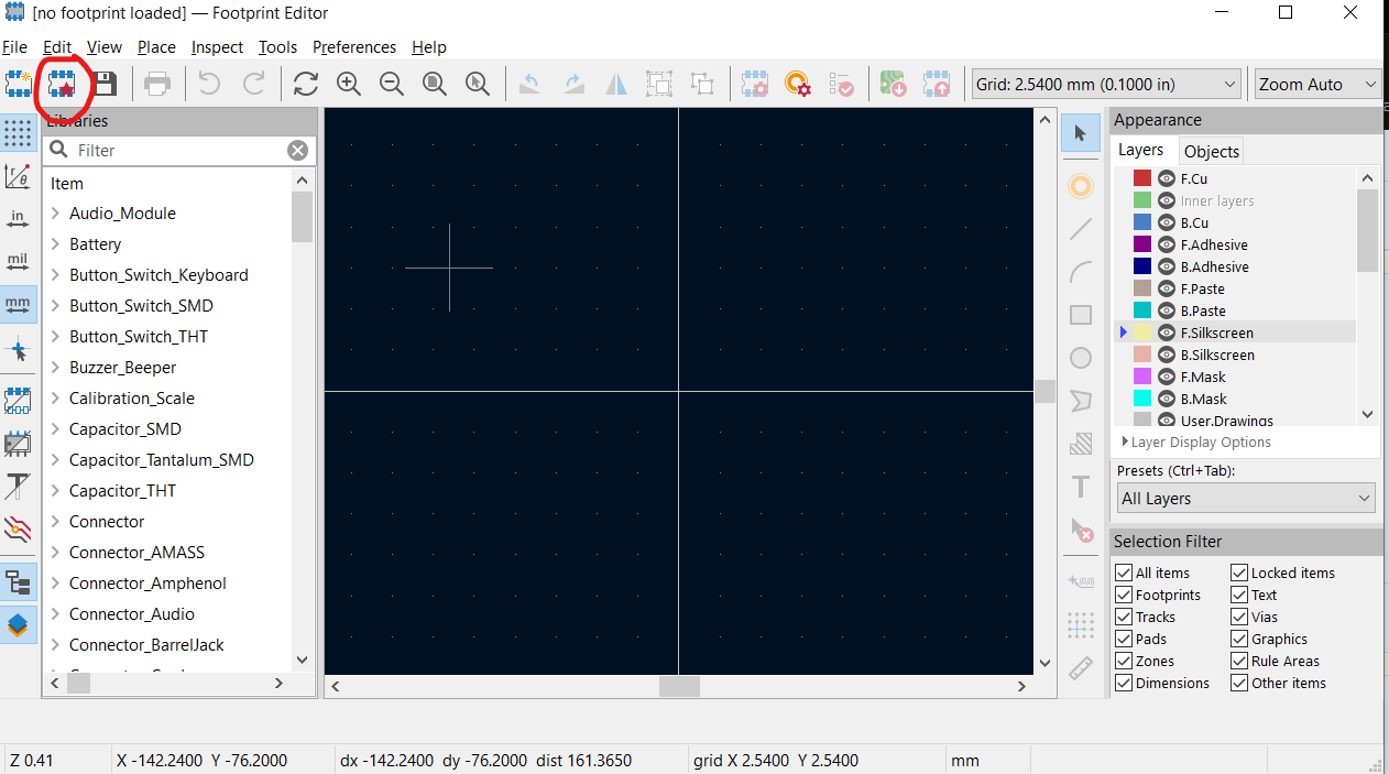 Figure
Select the S-DIP Single/Dual Package Footprint.
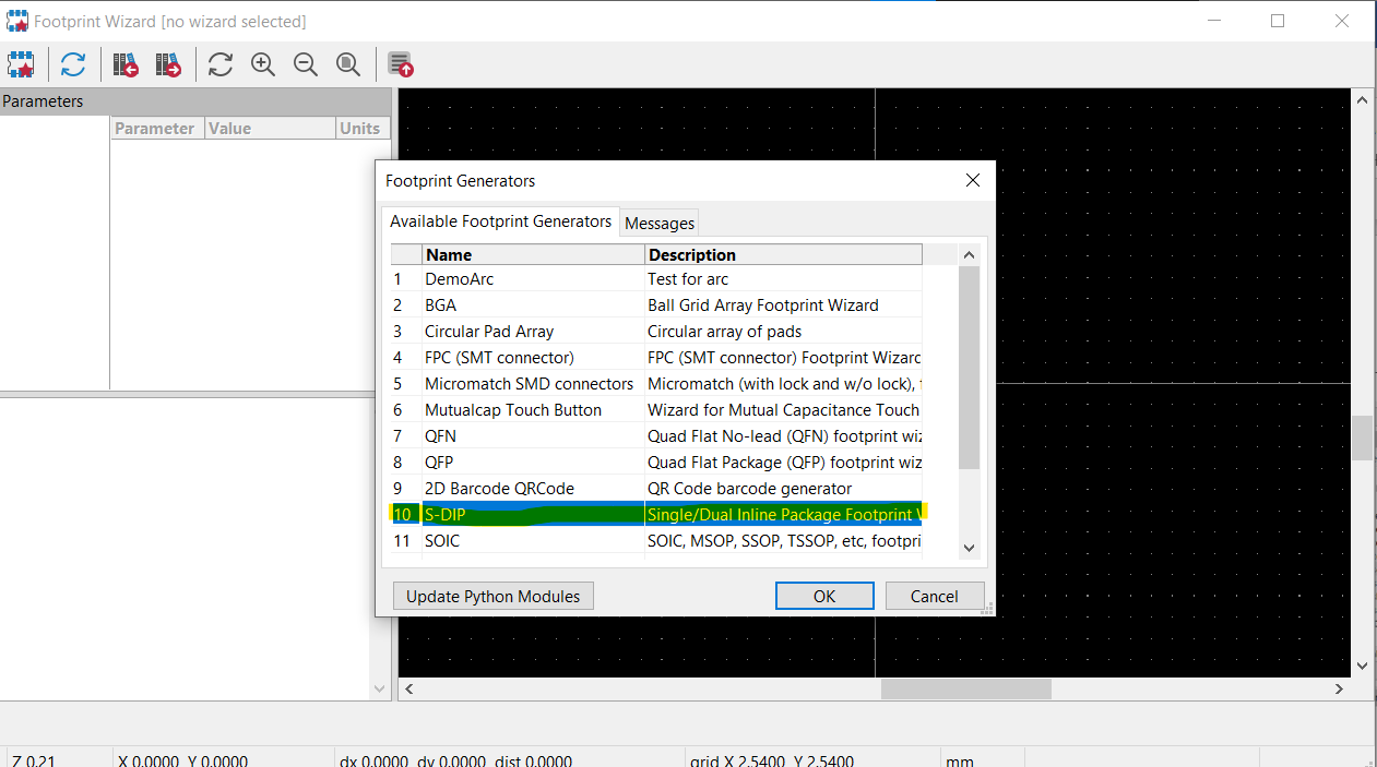 Figure
Adjust the pad count and row count parameter to match the number of pins on the LM317BT symbol.
Pad count, refers to the number of pins in each column. Row count, refers to the number of rows of pins.
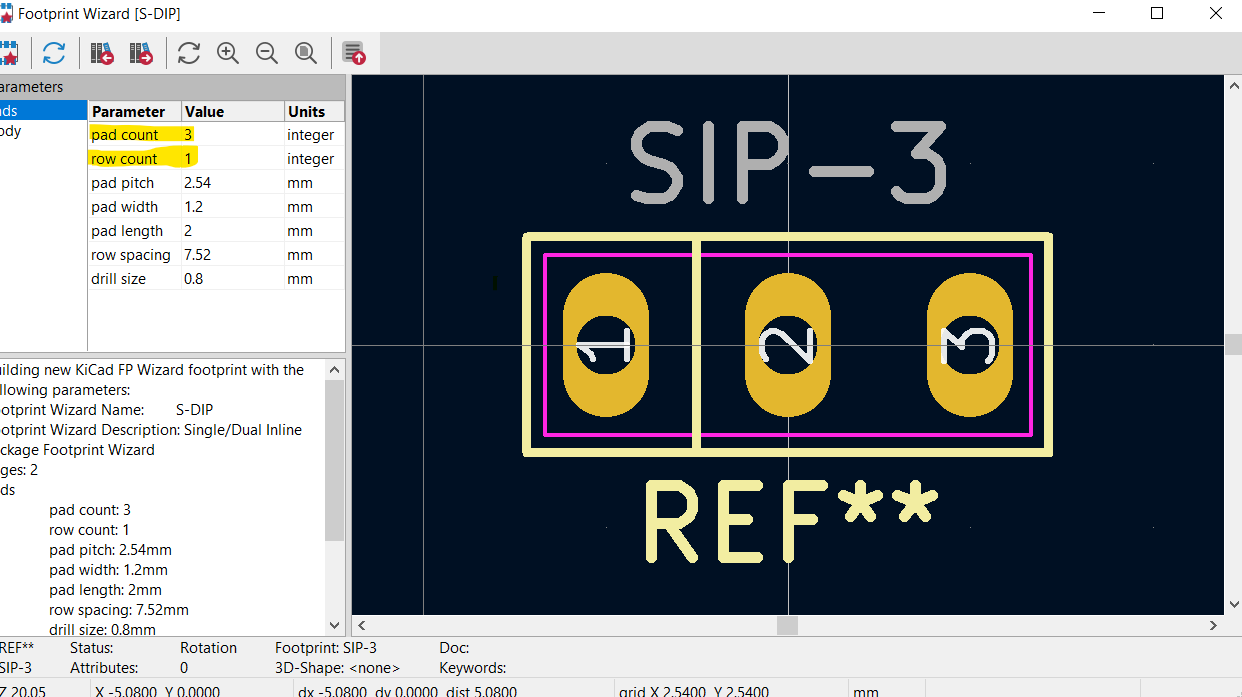 Figure
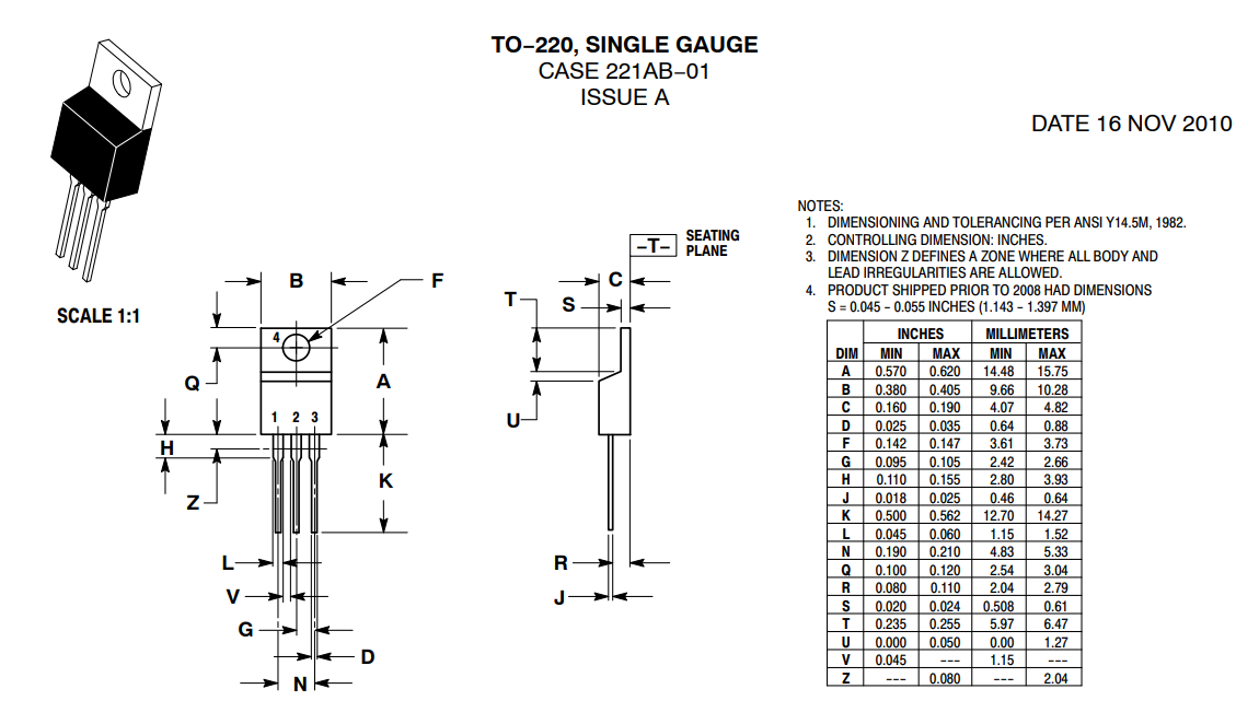
Now take a look at the datasheet for the TO-220 package the LM317BT regulator comes in. Find the Mechanical Case Outline that includes the package dimensions.
 Figure
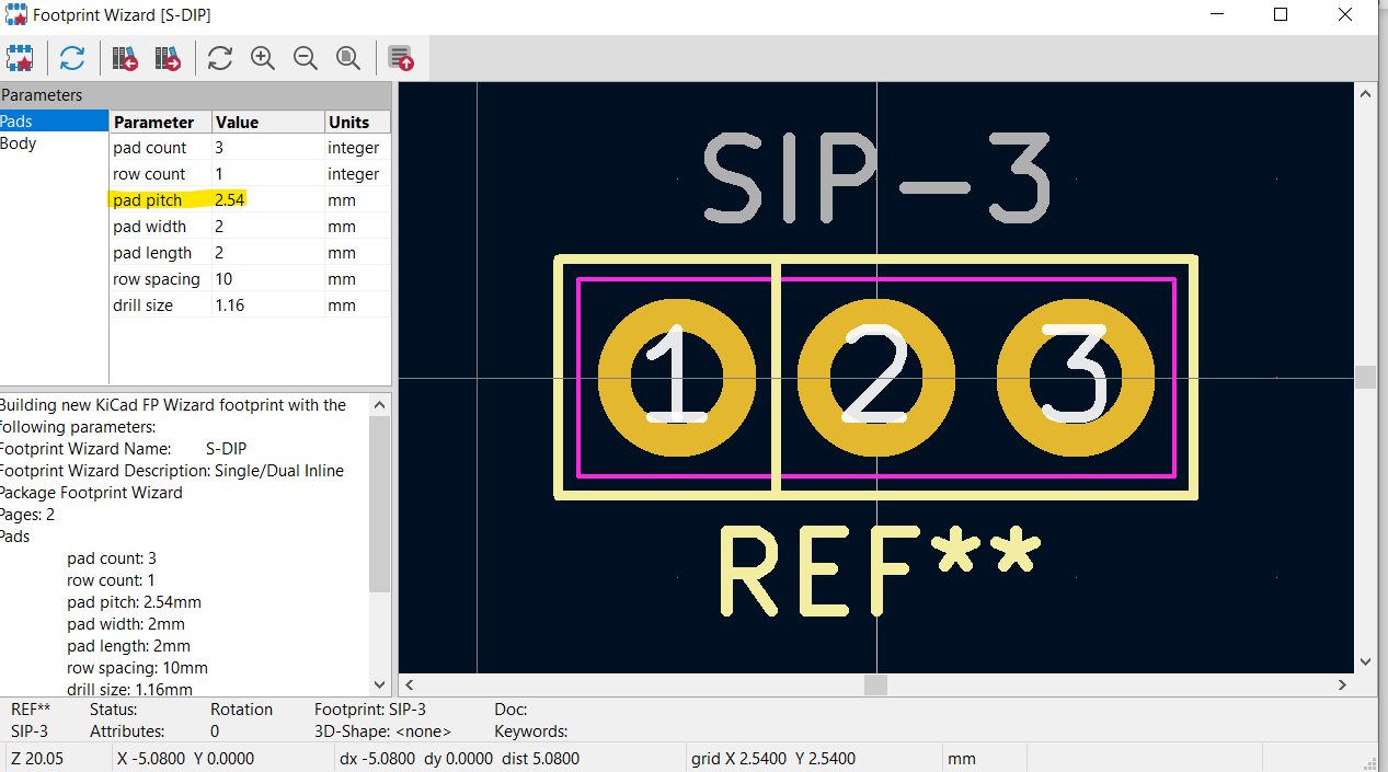
Variable “G” indicates pin pitch, with a minimum of 2.42mm and a maximum of 2.66mm. We will take the average to ensure the pin pitch is correct. The maximum pin pitch will be 2.54mm.
Adjust the pin pitch parameter in the footprint wizard to match step 6.
 Figure
Variable “D” indicates pin width, with a minimum of 0.64mm and a maximum of 0.88mm. We will take the average to ensure the pin width is correct. The maximum pin thickness will be 0.76mm.
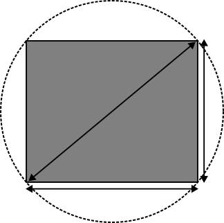
If the maximum width $w$ is 0.88mm and the maximum thickness t is 0.76mm, then the maximum possible hypotenuse $h$ is $h=\sqrt{(w^2 + t^2)}$, or 1.16mm. Setting the drill size to that maximum possible value will ensure all parts fit, though there may be some slop in standard parts. This ensures the tolerances on a given part fit the footprint.
 dimensions
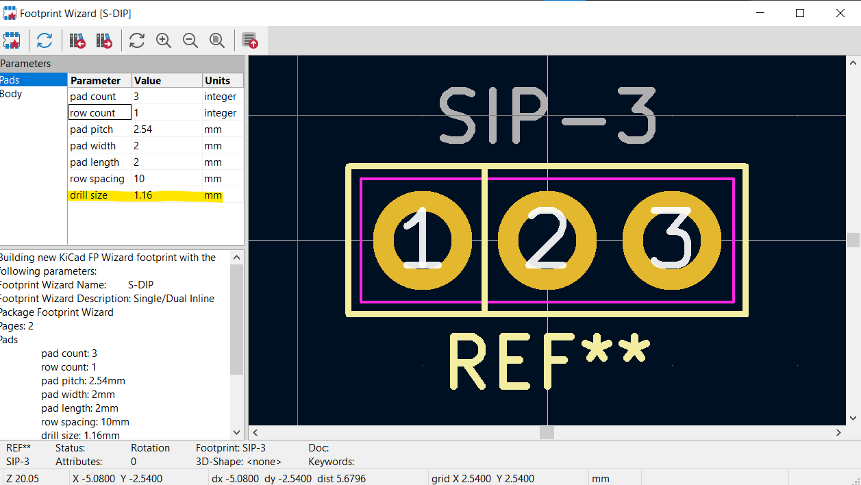
Adjust the drill size to the calculated value of 1.16mm.
 Figure
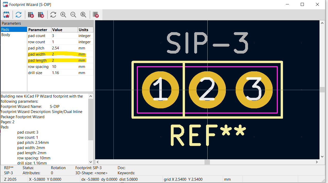
Adjust the pad width and length to desired values without creating overlapping pads.
Overlapping and small pads are bad practice and can lead to a short or the pads being stripped off of the PCB.* The DFM check (upcoming tutorial) will also help you understand your limits.
 Figure
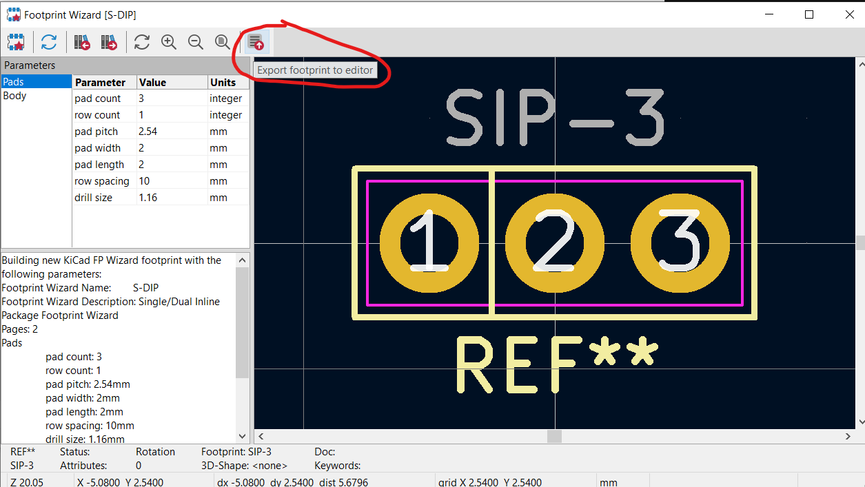
Export the footprint to the editor.
 Figure
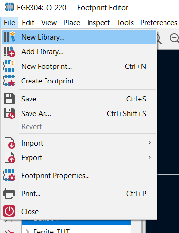
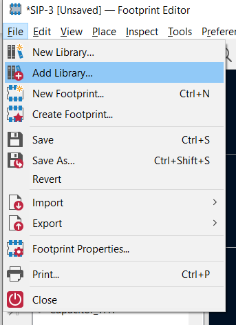
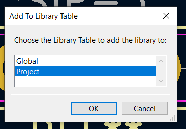
Create a new footprint library for your project.
 Figure
 Figure
 Figure
** It’s probably a good idea at this early stage in your PCB design career to associate your footprint library with your project. You may make different decisions later.
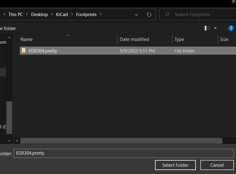
Select the library folder you generated.
 Figure
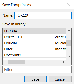
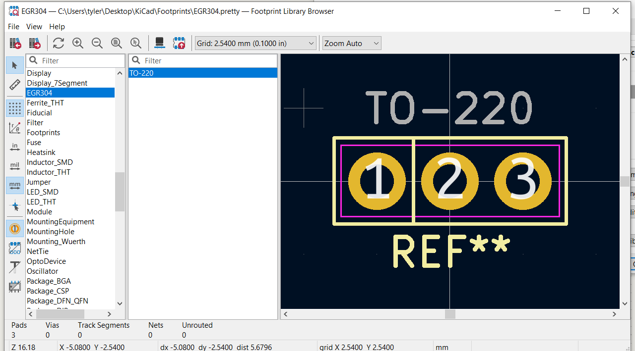
Save the footprint in the new footprint library.
 Figure
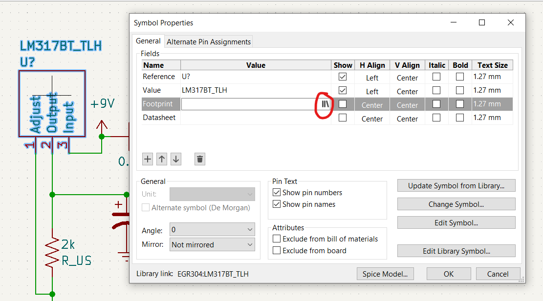
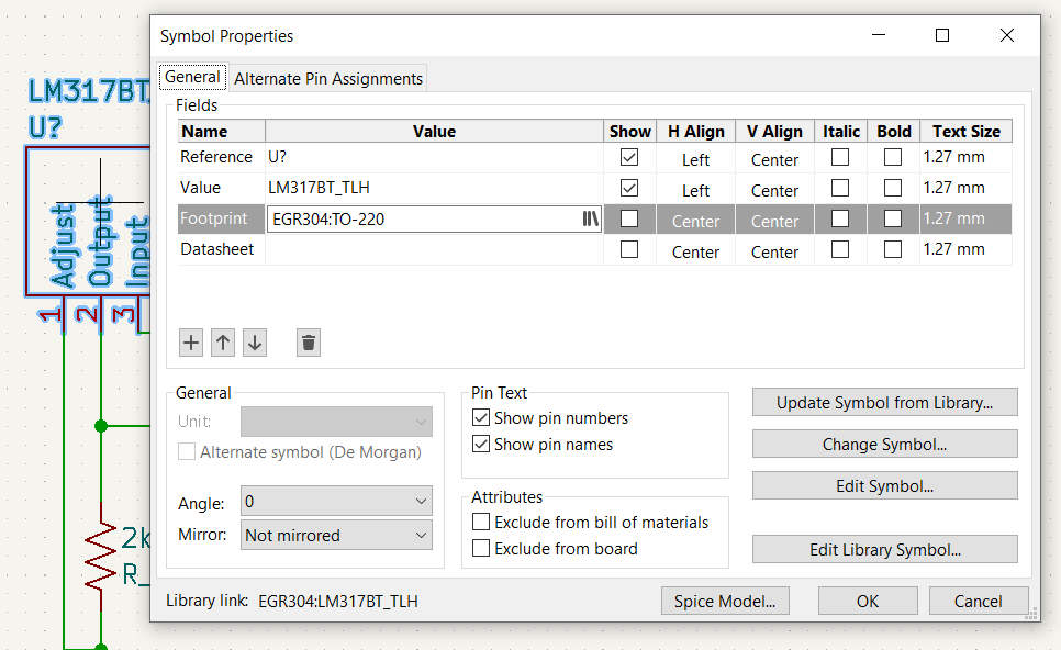
You can now go double click on your symbol and add the footprint!
 Figure
 Figure
 Figure
To show it working I imported my schematic into the PCB editor.*
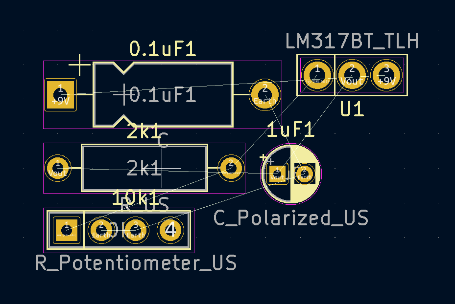 Figure